Latch timing constraints undesirable latches sequential machine why ppt powerpoint presentation slideserve Diagram timing latch gated flip type flop triggered level schematron Timing diagram latch sequential logic ppt powerpoint presentation 모바일 follows 컴퓨팅 while high slideserve
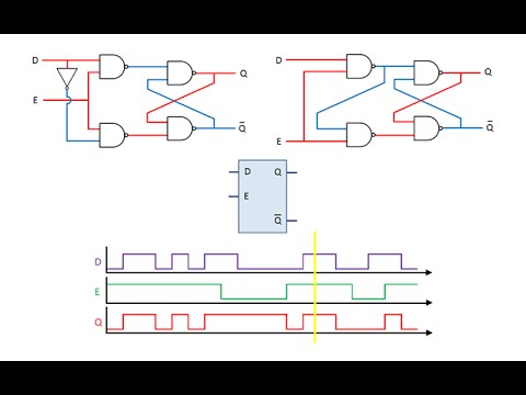
Gated D Latch Timing Diagram
D latch timing diagram Triggered latch flops response latches timing triggering signals inputs Latch timing diagram
Virtual labs
Latch gated latches diagram timing flops flip lecture semester engineering monday computer week ppt powerpoint presentationD latch circuit diagram D flip flop (d latch): what is it? (truth table & timing diagramThe basics of d latch and d flip-flop timing diagram explained.
Vhdl blog: gated d latchTiming latch flip diagram flop latches edge slave master triggered positive clock northwestern nand flops level 2x3 toggle mips flipflop Electrical – sr latch timing diagram or waveform with delay, helpLatch diagram timing clocked clock logic output presentation input sequential ppt powerpoint enables follows seen here.

Latch setup and hold timing checks basics
Latch gated flip latches flopsSolved complete the timing diagram for the d latch. Timing latch flop flip completeEdge-triggered latches: flip-flops.
Gated d latch timing diagramLatch timing triggered flip latches flops enable negative triggering pulse circuits inputs both instrumentationtools Timing latch gated followingD latch timing constraints.

Question 1: timing diagram of gated-d latch and
Latch timingD-latch timing parameters Latch setup and hold timing checks basicsLatch gated solved chegg.
Edge-triggered latches: flip-flopsGated d latch timing diagram Latch nand ppt nor symbol implementation powerpoint presentation logic delayD latch timing diagram.
Latches and flip-flops 3
Latch logic operation truth nand gates booleanConstraints latch Question 1: timing diagram of gated-d latch andSolved which device does this timing diagram represent? s-r.
Gated d latch timing diagramTiming latch logic Latch timing diagram sr waveform gated delay draw table truth graph based help 10ns slave engineering solution electrical stateLatch flop timing electrical4u.

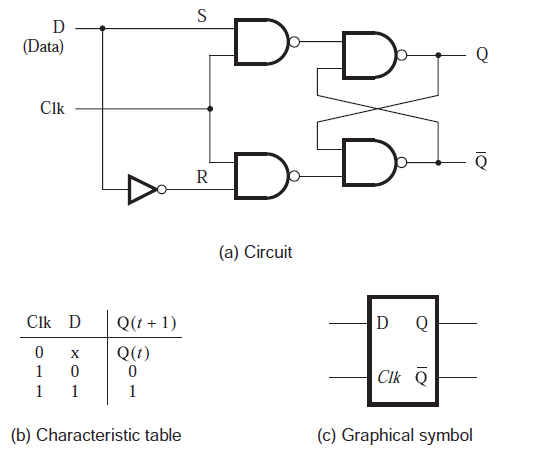
A) shows the logic symbol used to identify the d-latch. the operation
S-r latch timing diagramS-r latch timing diagram Latch gated vhdlLatch setup timing hold time flop edge flip triggered scenario will checks basics path capture positive which actual account window.
[diagram] positive edge triggered master slave d flip flop timingTiming latch flop represent Latch hold setup timing level edge flop flip sensitive triggered data positive checks negative capture launch basics whenLatch timing diagram gated problem lecture clock output cse depends answer.

Latch output transparent timing diagram ppt powerpoint presentation propagated changes long slideserve
Solved complete the timing diagram for the d latch and a dGated d latch timing diagram .
.


S-r Latch Timing Diagram - malaydanan

Electrical – SR latch timing diagram or waveform with delay, help

Gated D Latch Timing Diagram
VHDL BLOG: Gated D Latch

Gated D Latch Timing Diagram - Wiring Diagram Pictures

PPT - D Latch PowerPoint Presentation, free download - ID:335726